|
== Fabrication of CIGS "High Efficiency" Solar Cells ==
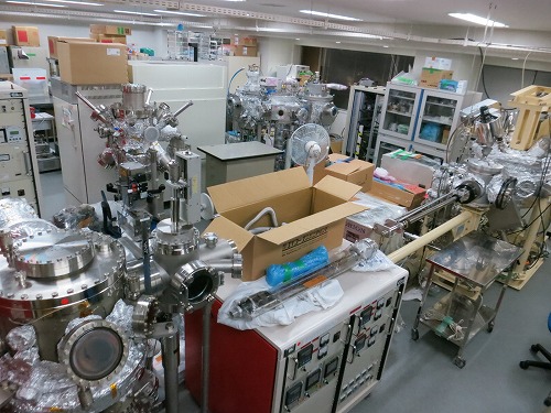
Even though researchers have made an
extraordinary progress Cu(In,Ga)Se2 (GIGS) solar modules over the years by
improving the performance significantly, low cost and reliability remain
major considerations and challenges. We are striving to produce a high
quality photoabsorbing layer and a windows layer with better
optoelectronic properties. Together, these films will increase the
efficiency of the solar cell devices. The ultimate of this research is to
transfer laboratory achievements to the commercial production; to
substantially affect the world of science and technology through these
advances.
More detail:
+
“Advantages of using amorphous indium zinc oxide films for window
layer in Cu(In,Ga)Se2 solar cells”, Thin Solid Films, 520 (2012)
2119-2122.
+ “Sulfurization Growth of CuInS2 Thin Film Using
Ditertiarybutylsulfide as a Less Hazardous Source”, Japanese Journal
of Applied Physics 50 (2011)065503.
+ “Growth of Cu(In,Al)(Se,S)2
thin films by selenization and sulfurization for a wide bandgap absorber”,
Japanese Journal of Applied Physics 50 (2011) 05FB07.
+ “Morphological and Structural Changes in
Cu(In,Ga)Se2 thin films by selenization using
diethylselenide”, Japanese Journal of Applied Physics 50 (2011)
05FB05.
== Fabrication of SnS "Earth abandant" Solar Cells ==
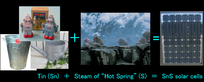
Our group has proposed “Earth abandant material used
solar cell” using a cheap and non-toxic materials such as binary IV-VI
orthorhombic semiconductor tin monosulfide (SnS). In fact, Sn and S
are abundant in the Earth’s crust; they have Clarke numbers of the order
of 31 and 15, respectively. Since these elements are safe for both the
environment and the human body, SnS is believed to be a safe
semiconducting material. SnS films have been deposited by
sulfurization, that is the most desirable because they can economically
deposit large-area films with well-controlled compositions.
More detail:
+ “Experimental determination of
vacuum-level band alignments of SnS-based solar cells by photoelectron
yield spectroscop”, Journal Applied Phys. 115 (2014)
083508.
+ “Sulfurization growth of SnS thin films and
experimental determination of balance band discontinuity for SnS-related
solar cells”, Japanese Journal of Applied Physics 50 (2011)
05FH03.
+ “Band Offset of SnS Solar Cell Structure Measured
by X-ray Photoelectron Spectroscopy”, Thin Solid Films, 519 (2011)
7249-7431.
== Fabrication of NiO "Invisible" Solar Cells
==
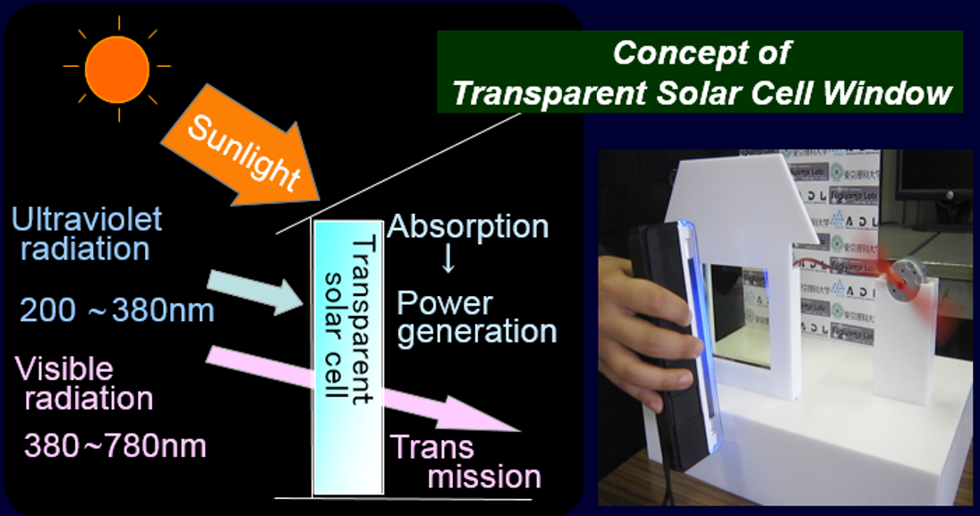
Our group has proposed “Invisible
solar cell” using a oxide semiconductors such as p-type nickel
oxide (NiO) and related n-type oxide films for fabrication of "transparent
solar cell window". Only UV light, which harmful to humans, absorbs the
NiO-related solar cell. Therefore, UV light is cut in the window and only
visible and infrared light, which is necessary for life, enter the room.
We have studied the crystal growth and characterization of NiO. We reveal
the advantages of using simple growth processes along with characteristics
of these solar cells.
More detail:
+
Experimental determination of band offsets of NiO-based thin film
heterojunctions”, Journal Applied Phys. 116 (2014) 163108.
+
“Fabrication of Visible-Light-Transparent Solar Cells using p-type NiO
Films by Low Oxygen Fraction Reactive RF Sputtering
Deposition”, Japanese Journal of Applied Physics, 52 (2013)
021102.
==
"Degradation Properties" of Solar Cells ==
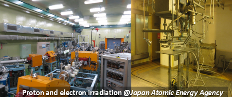
Nowadays,
much number of solar cells have been used. Fabrication skill and related
physics are well known. However, only a few degradation studies have been
conducted on the solar cells and composed thin films, which has resulted
in limited knowledge of both the mechanisms responsible for “how to
degraded” or “what part is weak” the solar cells. Our group have gradually
come to realize that the mechanism governing solar cell degradation is a
complex phenomenon under the proton- and electron-irradiated situation,
the sputtering damage during TCO deposition.
More detail:
.
+ Investigation of Sputtering Damage around pn
Interfaces of Cu(In,Ga)Se2 Solar Cells by Impedance
Spectroscopy”, Electrochimica Acta, 131 (2014)
236-239.
+ “Application of impedance spectroscopy to
investigate the electrical properties around the pn interface of
Cu(In,Ga)Se2 solar cells”, Thin Solid Films, 535 (2013)
287-290.
+ “Effects of Proton Irradiation on Optical and
Electrical Properties of Cu(In,Ga)Se2 Solar Cells”, Japanese Journal
of Applied Physics 51 (2012) 111802.
+ “Optical and electrical
properties of electron-irradiated Cu(In,Ga)Se2 solar cells”, Thin
Solid Films, 519 (2011) 7321-7323.
|